03/01/2020
Basic Technologies toward the All-Photonics NetworkTetsuomi Sogawa
Senior Vice President,
Head of NTT Science and Core Technology Laboratory Group
Feature Articles: NTT R&D Forum 2019 Special Sessions, NTT Technical Review, Mar 2020.
1. Introduction
Internet traffic continues to dramatically increase, resulting in more power consumed by information technology equipment called upon to process huge amounts of data. At the same time, Moore's Law, the scaling law involving the evolution of large-scale integrated circuits, is approaching its limit. The miniaturization of semiconductor devices generates leakage currents and heat, thus, degrades performance. Though the amount of data that must be processed continues to increase, the inability of scaling up computing power at its traditional pace is becoming a fundamental problem.
2. What is the All-Photonics Network?
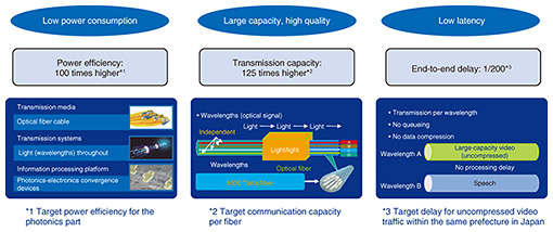
One target for the All-Photonics Network, a key element of Innovative Optical and Wireless Network (IOWN), is a 100-fold increase in power efficiency (Fig. 1). To this end, we are studying technology for transmitting signals using light from the network to terminals and studying new devices such as photonic-electronics convergence devices. We also aim to increase transmission capacity 125 fold, so we are studying large-capacity optical transmission system/device technology using, for example, new optical fibers such as multicore fiber. Furthermore, to reduce end-to-end delay by 1/200, we are researching various technologies to, for example, transmit information with no compression when communications do not allow for delay.
3. Role of increasingly important optical technology
Easy-to-use electronic technology has been used for chips that perform a variety of operations in computers. However, the recent trend toward high-density integration has been accompanied by an increase in the heat generated by wiring within a chip and the resultant constraint on performance. For this reason, we set as a target a new chip that integrates optics and electronics with lower power consumption by introducing optical communications technology in the chip's wiring section that incorporates high-speed computing technology characteristics of optical technology. Therefore, the use of optical technology in an end-to-end manner in conjunction with network opticalization plays an important role in making IOWN a reality.
This article focuses on four research themes toward achieving the All-Photonics Network.
4. Large-capacity optical transmission system/device technology
Compared with the 1980s when optical communications first got underway, communication speeds using optical fiber have increased by as much as six orders of magnitude over the last forty years (Fig. 2). This has been enabled by key inventions such as semiconductor lasers, planar lightwave circuits, and fiber amplifiers, and transmission capacity has recently dramatically increased through the development of digital signal processors for digital coherent communications.
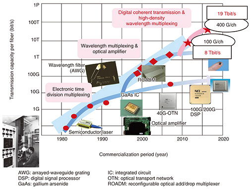
NTT reported in 2019 on a successful experiment to transmit 1 Tbit/s-per-wavelength optical signals in 35-wavelength division multiplexing at the laboratory level [1]. We also reported on the successful transmission of 1 Tbit/s-per-wavelength optical signals at a practical level for over 1000 km under a commercial environment using laid optical fiber [2]. The current outlook is for transmission on the level of 1 Pbit/s per fiber using, for example, a new fiber structure called multicore fiber that, as the name implies, incorporates many cores in a single fiber.
Devices applied to the core, metro, and access networks must evolve steadily, and devices that interconnect datacenters, the demand for which is growing dramatically, will become increasingly important. Therefore, there is a need for making as many end-to-end connections, including those between datacenters, as possible by optical means, and that is exactly what we want to achieve with IOWN.
5. Photonics-electronics convergence technology
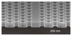
Although it was very difficult to handle light in the past, a structure called a photonic crystal (Fig. 3), in which the refractive index is changed periodically, has made it possible to confine light to a small area and improve the interaction between light and material. Basic low-power operation of a variety of devices based on photonic crystals, such as optical switches, optical lasers, optical memory, and optical random-access memory, has been demonstrated experimentally.
The roadmap for photonics-electronics convergence technology is shown in Fig. 4. In Step 1, the plan is to achieve a structure that integrates circuits mounted using silicon photonics with fibers, analog integrated circuits (ICs), etc. and achieve high connection speeds with elements outside the chip. In Step 2, the plan is to directly interconnect chips by short-range optical wiring, and in Step 3, the plan is to make inter-core connections within a chip by optical wiring to achieve ultra-low-power consumption.
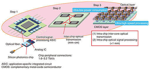
Step 3 will further improve the performance of chips by taking advantage of the arithmetic processing that is characteristic of light. While passing through a typical n-step logic gate would generate n-step worth of delay, the form of optical switches and optical circuit as a logic circuit, which we call an optical pass gate, can obtain a calculation result instantaneously with just the time taken to pass through the optical circuit [3]. Although we are at the basic evaluation stage with just a small number of bits, we are also studying the application of optical pass gates and optical transistors [4].
6. LASOLV™ coherent Ising machine
Next-generation computers, many of which have been announced in recent years, are expected to solve complex problems requiring a huge amount of computational resources that have been difficult with conventional computers [5], [6]. Against this background, we are researching solutions to combinatorial optimization problems-one type of complex problem-through the use of our coherent Ising machine called LASOLVTM that uses optical technology, one of NTT's main focus areas. There are many combinatorial optimization problems in the real world. They involve a massive number of combinations that are generated when the number of options increases, a situation that has been difficult with current computers.
Combinatorial optimization problems can be converted to graph problems, and an Ising machine is a computer based on the new concept of conducting physical experiments to derive solutions to such graph problems. For example, if we were to arrange a magnet oriented to either the S-pole or N-pole at each node of a graph according to certain constraints then release our hold on those magnets, the total energy of the system would take on its smallest value as the magnets orientate themselves to their most stable configurations. This would, in effect, derive an answer to that graph problem.
LASOLV uses optical technology to create a situation equivalent to this magnet experiment. Specifically, it inputs 2000 optical pulses into an optical fiber 1 km in length and passes them any number of times through a special optical amplifier to amplify them repeatedly. The system eventually settles into a state whereby the phase of each optical pulse is either 0 or π. If we compare the oscillation of an optical wave to that of a playground swing, we can say that it settles into a state whereby the swing is either ahead or behind. In addition, the machine takes some of the optical pulses from the optical fiber and measures their phase states, sets constraints in the graph problem in terms of optical interactions, and returns these pulses to the optical fiber overlaying them on the original pulses. Repeating this process while circulating the optical pulses about 1000 times through the optical fiber provides a solution to the problem (Fig. 5)
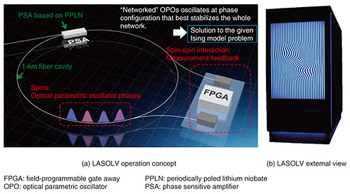
On comparing LASOLV with quantum annealing developed by another company, it was found that LASOLV exhibited superior performance the more complex the graph structure became, even when solving relatively small problems. It has also been recently found that LASOLV can even be useful in solving larger-size problems [7].
LASOLV can be applied to complex wavelength-allocation problems in the All-Photonics Network of IOWN and perform high-load processing in machine learning.
7. Optical lattice clock network
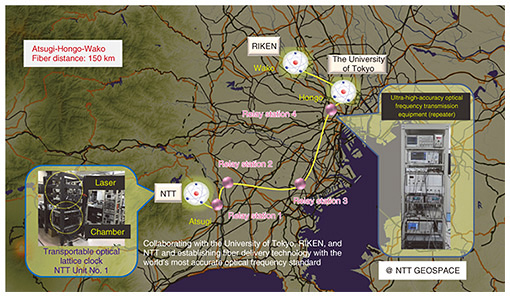
The optical lattice clock invented by Professor Hidetoshi Katori of the University of Tokyo loses only one second every 30 billion years, which is more accurate than the advanced cesium atomic clock by three orders of magnitude. The optical lattice clock can also be read out by laser, which opens up the possibility of clock transmission over optical fiber. We are studying what this feature has to offer by constructing a network of optical lattice clocks installed in many of NTT's central offices.
As suggested by the general theory of relativity, clocks run faster at higher altitudes, so optical lattice clocks that have achieved 10-18 of total accuracy of clock frequency allow us to compare remote locations and measure differences in altitude as small as 1 cm. In Japan, an earthquake-prone country, this means that minute crustal movements and massive gravitational movements can be detected, which points to the possibility of constructing a very effective, safe, and secure infrastructures.
However, when carrying such ultra-high-accuracy signals by optical fiber, it is necessary to control drops in accuracy caused by optical fiber fluctuations. We are currently conducting a trial of an optical lattice clock network that connects various bases by NTT EAST optical fiber and includes relay equipment installed in NTT central offices (relay stations) to cancel such optical fiber fluctuations while maintaining high accuracy (Fig. 6). In the future, we would like to see an optical lattice clock network introduced into IOWN for developing new types of time-related business.
8. Toward Achieving the All-Photonics Network
Going forward, we will promote research and development efforts to achieve world-best, world-first, and impressive technology. We will promote further research and development of photonics-electronics convergence technology, the key to achieving the All-Photonics Network.
We also plan to make IOWN a reality in collaboration with experts in a wide array of research and technology fields while holding discussions with various companies and universities via the IOWN Global Forum [8]. To all parties involved in this effort, we look forward to your support and cooperation.
References
- [1]Press release issued by NTT on Mar. 7, 2019 (in Japanese),
https://group.ntt/jp/newsrelease/2019/03/07/190307a.html - [2]Press release issued by NTT, "Long-distance Transmission of 1 Tbit/s Ultra-high-capacity Optical Signal-World record 1,122 km transmission in a commercial environment," June 19, 2019,
https://group.ntt/en/newsrelease/2019/06/19/190619a.html - [3]A. Shinya, T. Ishihara, K. Inoue, K. Nozaki, and M. Notomi, "Ultralow-latency Optical Circuit Based on Optical Pass Gate Logic," NTT Technical Review, Vol. 16, No. 7, 2018.
https://www.ntt-review.jp/archive/ntttechnical.php?contents=ntr201807fa6.html - [4]Press release issued by NTT on Apr. 16, 2019 (in Japanese),
https://group.ntt/jp/newsrelease/2019/04/16/190416a.html - [5]Google AI Quantum,
https://ai.google/research/teams/applied-science/quantum/ - [6]D-Wave,
https://www.dwavesys.com/ - [7]Press release issued by NTT on May 25, 2019 (in Japanese),
https://group.ntt/jp/newsrelease/2019/05/25/190525a.html - [8]IOWN Global Forum,
https://iowngf.org/